Ganglion Specs
BUY IT!
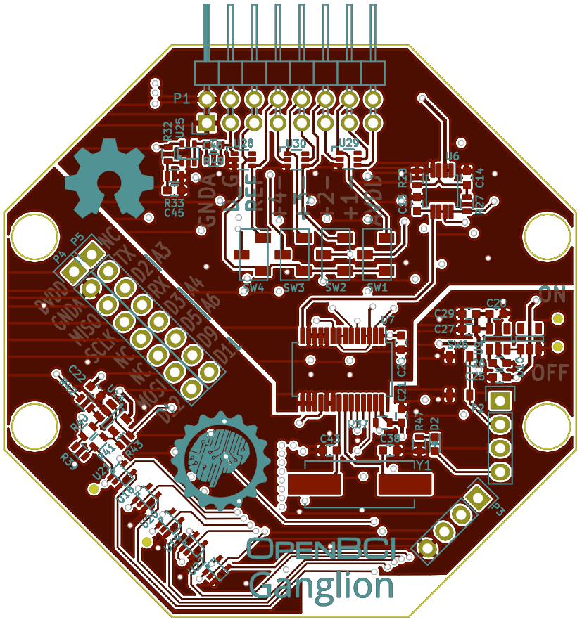
The OpenBCI Ganglion PCBs were designed with KiCAD, an open-source PCB capture software. You can find a link to download KiCAD in our Ganglion design files repository, where you will find design files and component library files to load into KiCAD and edit, if you like, along with the full BOM for this maiden production run.
OpenBCI Ganglion Board
Ganglion Board Specs
- Voltage resolution = 0.1788 microvolt/bit (3V/16777216)
- Resolution = Voltage level / 2^n, where n is the bit-level of the ADC
- Power with 3.3V to 12V DC battery ONLY
- Current Draw: 14mA when idle, 15mA when connected and streaming data
- Simblee BLE radio module (Arduino compatible)
- MCP3912 analog front end
- LIS2DH 3-axis accelerometer
- MicroSD card slot -- Not supported
- Board dimensions: 2.41" x 2.41" (octagon has 1" edges)
- Mount holes are 1/16" ID, 0.8" x 2.166" on center
- Switches to manually connect/disconnect inputs to the REF pin
Simblee Breakout Pins:
- Digital I/O Pins:
- D0, D1, D2, D3, D4, D5, D9, D11, D12, D21, D23, D24
- Analog Input Pins:
- A3, A4, A5, A6
- SPI bus pins:
- MOSI, MISO, SCK
- Other Pins:
- Simblee Reset, VDD, GND
The SPI pins are available for user access. The blue LED on the board is connected to pin D23. Note that the analog pins are shared with digital I/Os. VDD is 3.0V.
Push Button
The button switch is connected to the Simblee reset pin, along with a 10K pullup resistor. Pressing this button will put the Simblee into reset.
Sensor Input Header
The Ganglion Board is a 4 channel biosensing board. There is a 16 pin Right Angle header, which can be used to interface electrode sensors of all types. The inputs pins connect to an AD8237 InAmp buffer. This amplifier had differential inputs. the + input is called non-inverting, and the - input is called inverting. Here is a description of the pins.
GNDA- Power Supply: 0 Volts. Connects to the top and bottom pin
D_G- Driven Ground: 1.5 Volts. Connects to both the top and bottom pin
REF- Combined Reference input. Connects to the top and bottom pin
+4-- Channel input #4.
+input on top,-input on bottom
- Channel input #4.
+3-- Channel input #3.
+input on top,-input on bottom
- Channel input #3.
+2-- Channel input #2.
+input on top,-input on bottom
- Channel input #2.
+1-- Channel input #1.
+input on top,-input on bottom
- Channel input #1.
AVDD- Power Supply: 3.0 Volts Connects to the top and bottom pin
Both the schematic and layer diagrams show that top and bottom pins of D_G and REF are connected together with traces. So makes no difference which you use.
Inverting Input Select Switches
Each input channel is buffered by an AD8237 Instrumentation Amplifier with a differential input impedance of 100 MΩ. There are 4 small slide switches (SW1, SW2, SW3, SW4) which can be set to connect the - inputs from the InAmps either to their associated - pin, or to the REF pin.
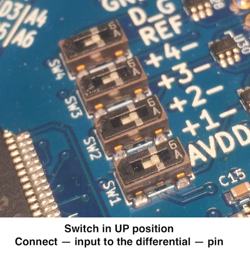
The default position for these switches when they are shipped to you is UP, which connects them to their associated differential channel - input pin on the bottom row of headers.
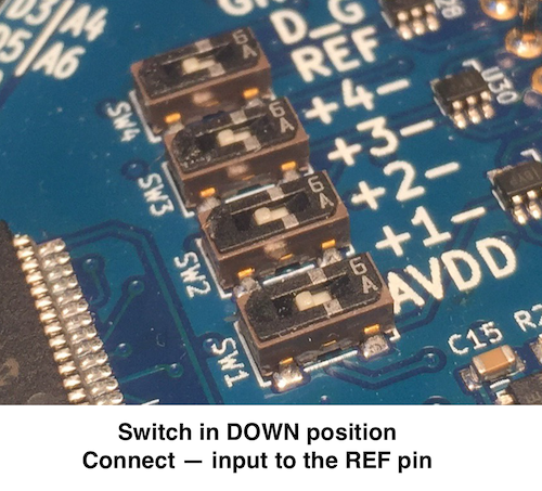
When you move the switch DOWN, that associated channel's - input is connected to the REF pin. This allows you to 'gang' some or all of the - pins together if you are doing something like reading EEG, or have any reason to combine two or more of the - pins.
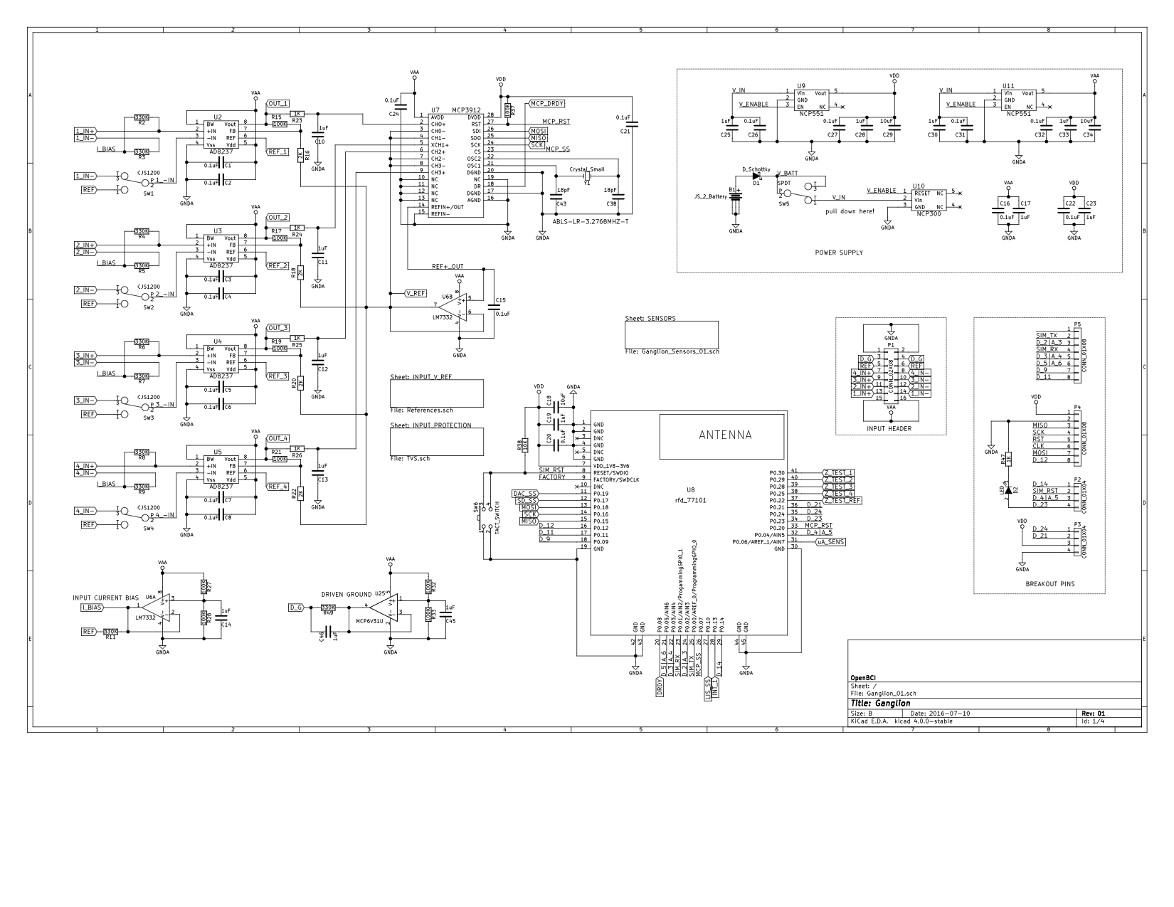
Ganglion Board Circuit Schematic
This is only the first page of the schematic. Download The Entire Schematic here
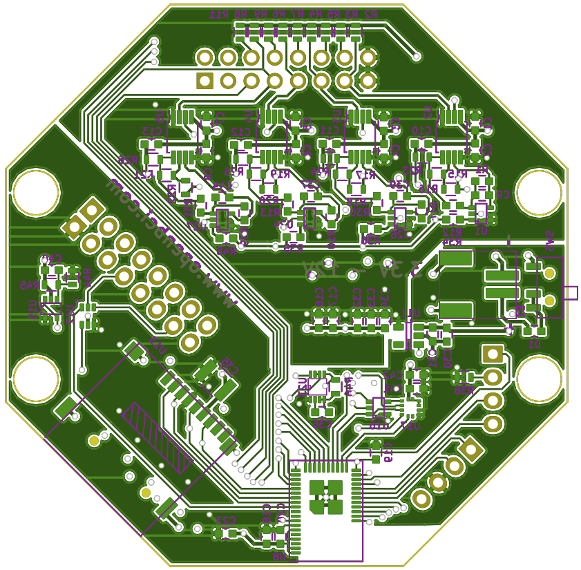
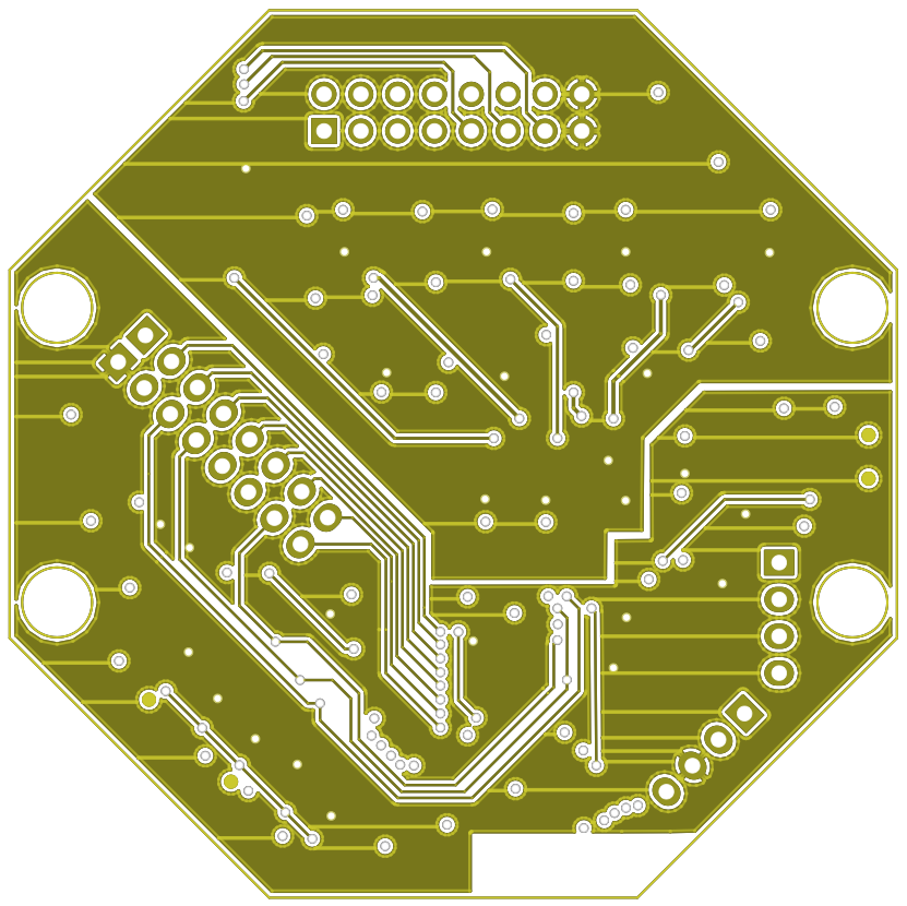
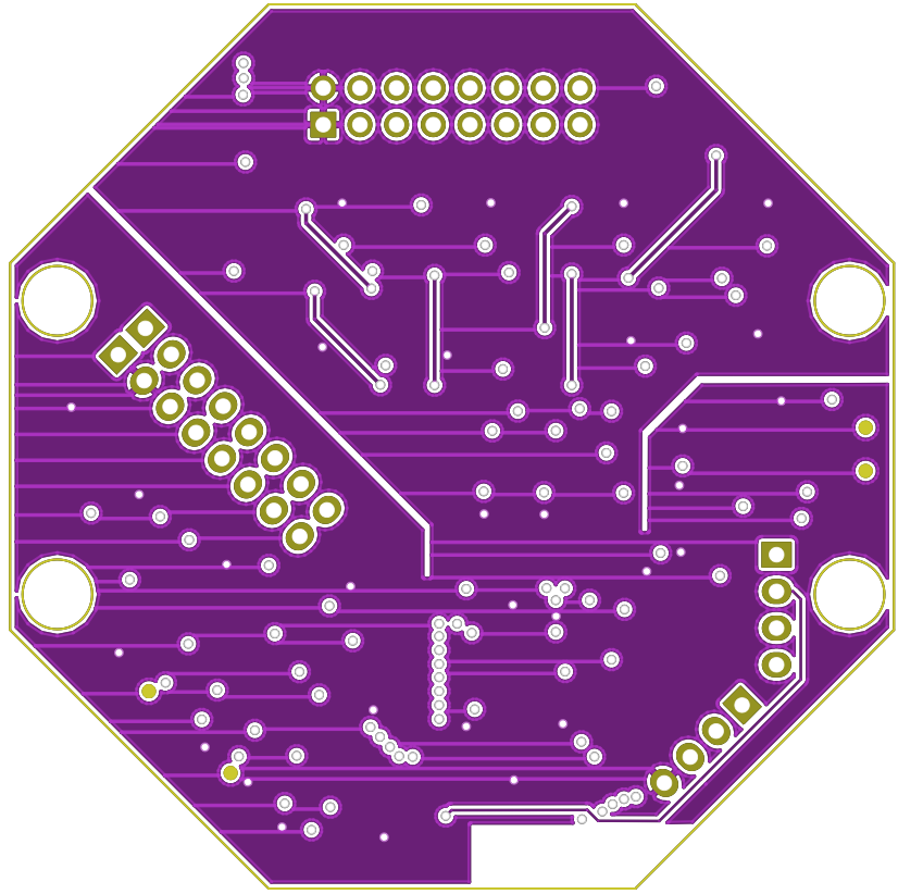
Ganglion Board PCB Layer Images
Top Layer
Inner Layer 1
Inner Layer 2
Bottom Layer